
Eye tracking technology for XR headsets is developing rapidly. One technique for tracking eye movements and determining the direction of a user's gaze includes analyzing infrared light signals directed toward and reflected from the user's eyes. For example, a head-mounted display can be equipped with one or more infrared light sources that emit infrared light from different directions toward the user's eyes. The infrared light (flicker) reflected from the user's eyes can be detected by a sensor and used to determine the XYZ position and gaze direction of the user's eyes.
In order to improve the accuracy and processing power of infrared eye tracking systems, it is usually necessary to place several different infrared light sources around the user's eyes to produce different flickers on the cornea.
Unfortunately, conventional XR systems have certain limitations in the positioning of infrared light sources. In particular, conventional systems have historically positioned infrared light sources at the peripheral edges of the headset or other structures where the actual display lenses and screens are mounted. This peripheral positioning of infrared light sources is not always optimal and requires the use of more light sources and/or larger, more powerful light sources. If the light source can be placed closer or more optimally relative to the iris of the user's eye, no additional light sources are required.
Some XR systems attempt to position infrared light sources away from the edge of the display and within the user's field of view to be close to the eyes. However, existing systems of this type are problematic because they create visual obstructions to the user's view of the mixed reality environment. In particular, existing infrared light sources are typically sized in the range of 1.0 mm to 4.0 mm in diameter/width. Such sizes are very noticeable, especially when positioned in the user's field of view. For at least this reason, most conventional systems position infrared light sources only in suboptimal locations at the peripheral edges of the lens/display.
Given this problem, Microsoft's patent application titled "Microled based invisible illumination for eye tracking" proposes a solution. In particular, Microsoft states that the invention allows infrared light sources to be positioned directly within the viewing area of the head-mounted display lens in an optimal orientation relative to the user's eye/iris and corresponding camera sensor, while not obstructing the user's perception of the mixed reality environment.
The company states that the approach is to utilize an illumination lens structure with infrared μLEDs that are less than 100 μm in any given direction, because even if embedded in the lens of the head-mounted display, the user cannot perceive such uLEDs, so they will not obstruct or interfere with the head-mounted display's presentation of the mixed reality environment during use.
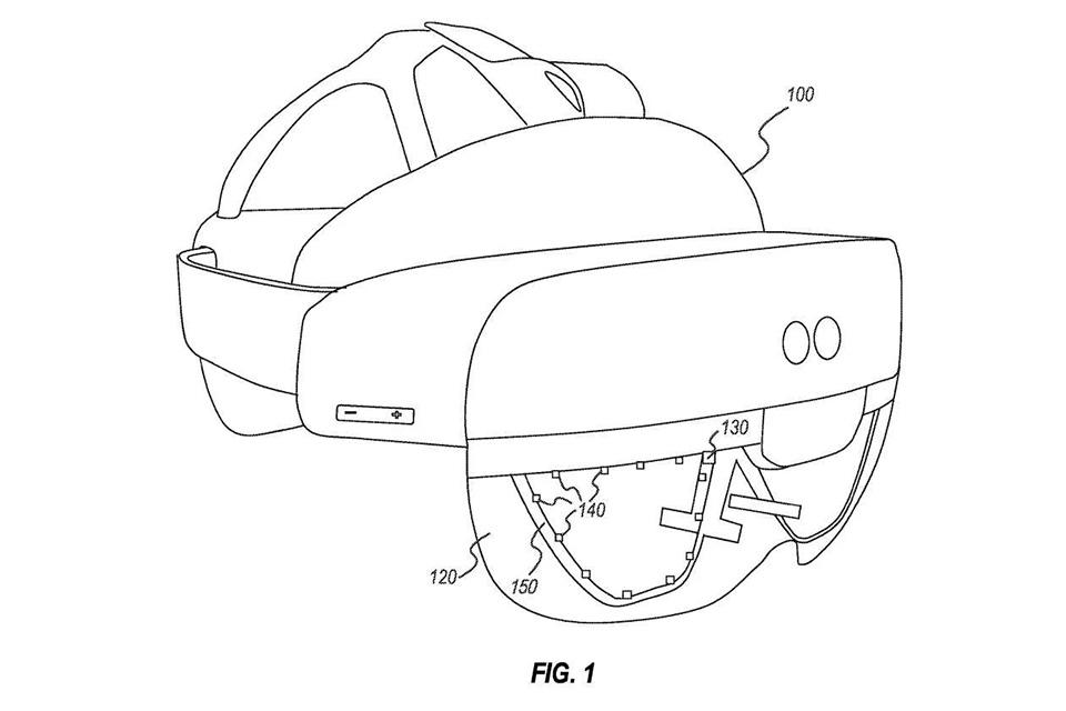
Now turning attention to FIG1 , the HMD is configured to perform eye tracking based on light reflections (glints) captured by camera 130 or other sensors. For example, during use, light is emitted from a light source around the user's eyes (. After the light is emitted, the flash is reflected from the user's eyes (particularly the user's iris) and detected by the camera.
Based on the perceived intensity/strength of the light, relative to the source/time when the light was emitted, the head display light processing module can detect the positioning (relative position and direction) of the user's eyes/irises.
Additional processing of the images captured by the system camera/sensor can be used to distinguish between the user's pupil and iris. Such images can help the system map the position of the user's eyes and the direction/gaze of the user's eyes relative to the projected hologram or other object. The system can also use the position of the user's eyes to support mixed reality environments, positioning and re-projecting holograms at desired locations.
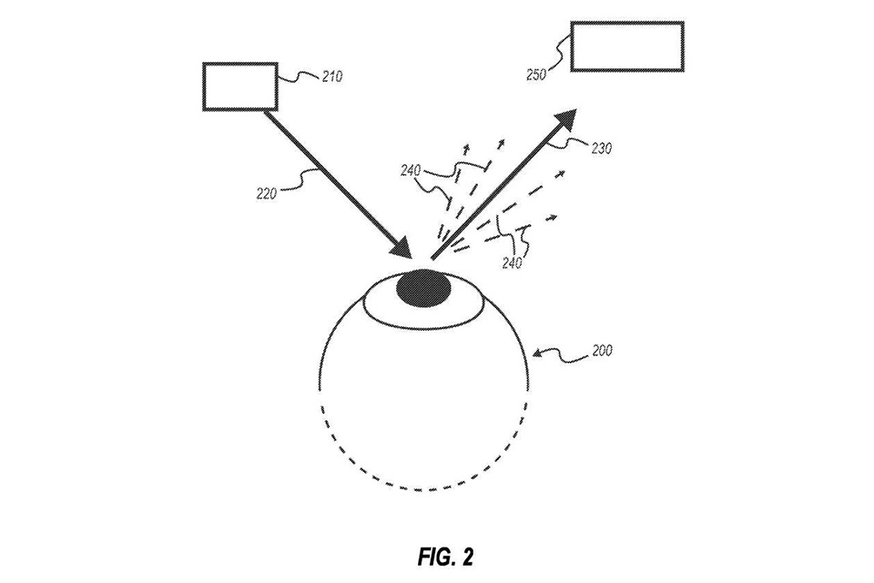
Figure 2 shows a representation of a user's eye 200, where an infrared light source 210 emits infrared light 220 toward the user's eye 200. The infrared light reflects back as specular reflections and diffuse reflections. Figure 2 also shows how a camera 250 or other sensor can be placed to detect one or more reflections.
By the position of the light source, the time when the light source emits the light, the position of the camera, and the measured intensity and time of the detected light reflection reflected from the user's eyes, the system can determine the relative positioning of the user's eyes/irises. This is because the light The light reflects differently in different parts of the user's eye, for example it reflects differently in the pupil and iris areas of the cornea than in the sclera. This difference is detected and measured based on whether the reflection is specular or diffuse.
In order for the light source to be optimally positioned, such as close to the user's cornea, it is necessary to position the light source in an appropriate location. Unfortunately, traditional infrared light sources are too large (e.g. 1-4 mm) to be positioned within the user's field of view without obstructing the user's view of the environment through the lens.
To help address these issues, Microsoft has proposed the use of an illumination lens configured with an infrared μLED. With this configuration, The light source is optimally placed close to the user's eyes without having to consider existing limitations imposed by the physical form factor of the head-mounted display mounting structure.
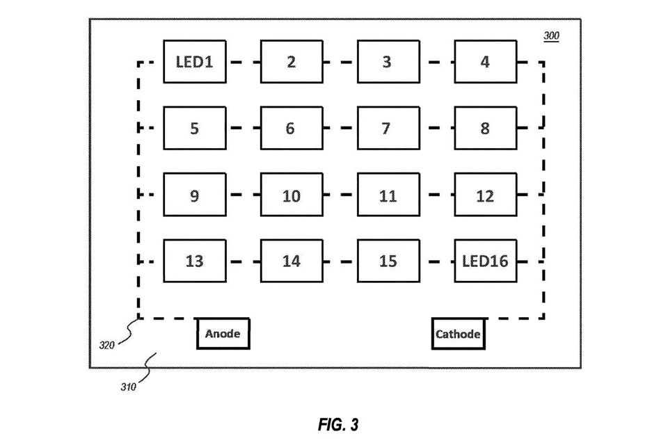
Figure 3 shows an infrared μLED lens structure 300 with 16 infrared μLEDs arranged in a grid. The infrared μLEDs are placed on a transparent substrate 310 and form a circuit between the anode terminal and the cathode terminal along a conductive trace 320. For example, when the circuit is powered by a power supply of the head-mounted display, the power supply can be electrically connected to the anode and cathode terminals and controlled by a lighting control unit, the infrared μLED will activate and emit infrared light.
The infrared μLED has an emission wavelength of 790 μm ~ 1mm. In a preferred embodiment, the infrared μLED emits light with a wavelength of about 800-900 μm, and even more preferably emits light with a wavelength of about 850 μm.
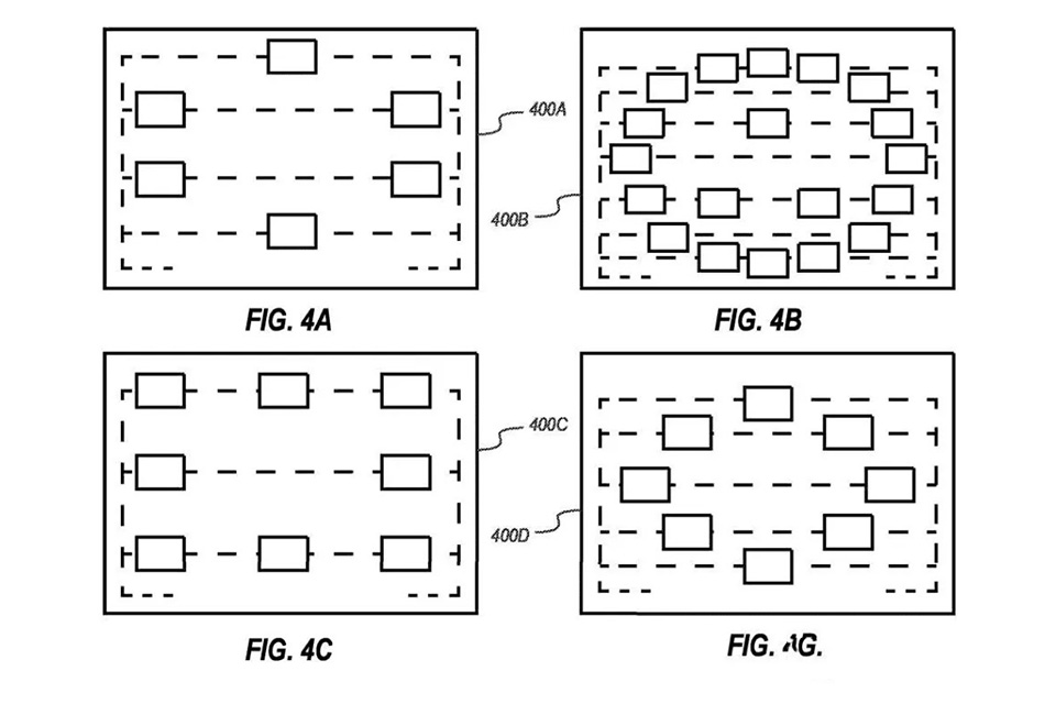
Figures 4A-4D show different numbers of infrared μLEDs in different illumination lens structures. Specifically, in Figure 4A, the distribution pattern of the infrared uLEDs is somewhat circular/elliptical, but somewhat rectangular in Figure 4C and somewhat diamond-shaped in Figure 4D. On the other hand, the embodiment shown in Figure 4B includes two different patterns, a circular/elliptical outer pattern and a triangular inner pattern.
In addition, the illumination lens structure 400A is composed of 6 infrared uLEDs, while the illumination lens structures 400C and 400D are each composed of 8 infrared uLEDs. The illumination lens structure 400B includes 19 infrared uLEDs.
The different numbers and patterns of infrared uLEDs can be changed to suit different needs and preferences.
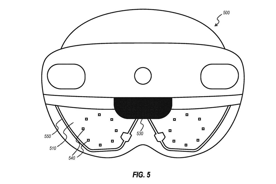
In Figure 5, the head display 500 is configured with a transparent illumination lens structure 510 having a plurality of infrared μLEDs 540. As shown, the infrared μLEDs 540 are arranged in a circular pattern, with eight for each eye and lens region. The different infrared μLEDs 540 may be selected to be connected to a single circuit or to two or more different circuits. The electrical traces forming the circuits are not shown.
During use, light emitted from the infrared uLEDs will be directed at least partially toward the user's eyes, and the light will be reflected back and detected by the device camera 530.
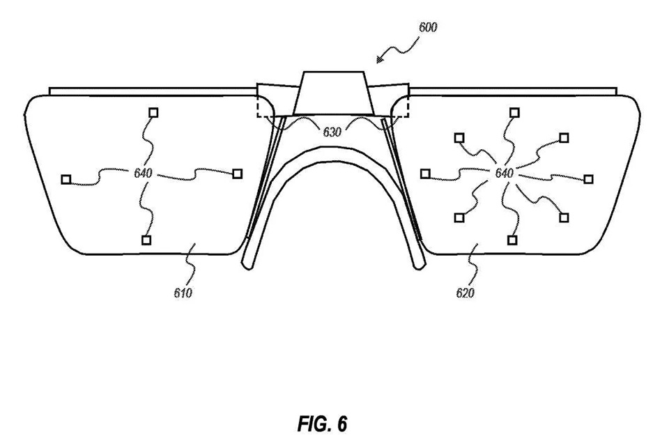
Figure 6 shows an embodiment of a pair of glasses 600 having a first transparent illumination lens structure 610 including four infrared uLEDs and a second transparent illumination lens structure 620 including eight infrared uLEDs.
This example is used to illustrate that the two sides of the headset do not necessarily have to have matching/symmetrical infrared uLED distributions. Regardless of the infrared uL Regardless of the number and distribution of EDs, it should be understood that during use, light emitted from the infrared uLEDs will be directed at least partially toward the user's eyes, and the light can be reflected back and detected by the device camera 630.
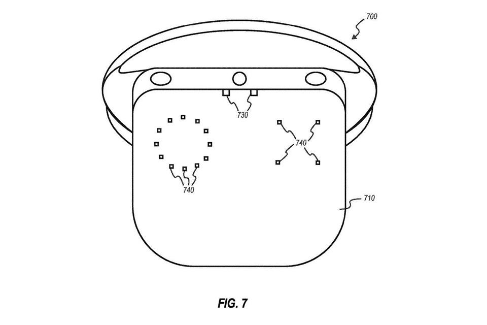
In a related embodiment, the head-mounted display system 700 shown in Figure 7 includes a transparent illumination lens structure 710 with a visor. In this example, there are several infrared uLEDs on one side of the visor forming a circular pattern. There are four infrared uLEDs on the other side of the visor, distributed in a square.
As with all previous examples, the infrared uLEDs are not shown to scale. In fact, the infrared uLEDs are so small (<100 μm) that, like the thickness of the traces, they would not be visible in the current illustrations if they were shown to scale.
Also because the infrared LEDs are so small, they can be used to illuminate the user's eyes with infrared light and simultaneously be positioned in the lens through which the user passes without obstructing the user's field of view through the lens.
The conductive traces are very thin, with a width of less than 50 μm, or even less than 25 μm, so when used close to the user's eyes, they are not visually obvious and are basically invisible. This configuration is particularly advantageous in enabling the traces to be positioned inside the illumination lens structure. Even if it is positioned directly in front of the user's eyes, it will not hinder the user's view of the environment perceived through the lens during use.
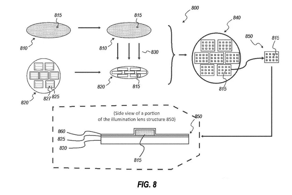
Figure 8 visualizes the manufacturing process for manufacturing the illumination lens structure of the invention.
As shown in the figure, the manufacturing process includes obtaining a wafer 810 containing one or more infrared μLEDs. For example, wafer 810 can be an epitaxial wafer formed by an epitaxial growth or deposition process.
The process 800 shown in Figure 8 also includes obtaining a substrate 820 for transferring the infrared uLEDs thereto. As shown in the figure, a transfer process 830 is performed to transfer one or more infrared uLEDs to conductive traces 825 that are already located on the substrate 820 and form one or more different circuits 827 on the substrate.
The size of the infrared μLED removed from the substrate and placed on the substrate is limited to <100 μm in any direction, so the maximum dimension of any measurable length of the infrared μLED is less than 100 μm.
The maximum dimension of the infrared uLED can be less than 75 μm, less than 50 μm, or even less than 20 μm. In one embodiment, the maximum size of the infrared uLED is about 10 μm.
The width of the trace is also limited, and the thickness cannot be greater than <50 μm, <40 μm, <30 μm, or even less than 20 μm. In one embodiment, the trace width is about 20 μm.
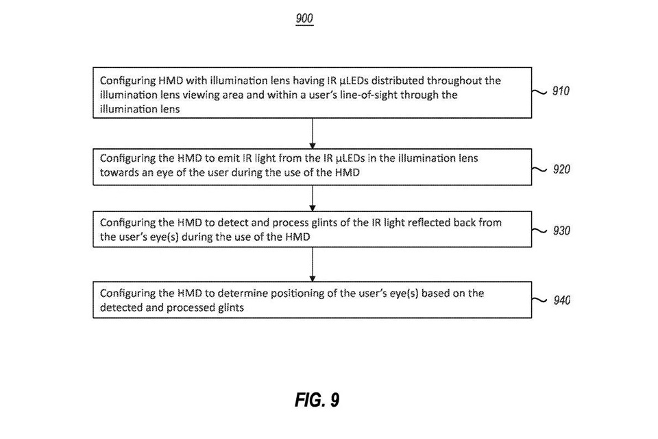
Figure 9 shows a flowchart 900 configured to perform eye tracking, wherein the head display includes an illumination lens including a plurality of infrared μLEDs, and each of the plurality of infrared μLEDs has <100 μm maximum size.
The system component controls the illumination of the infrared uLEDs, emitting infrared light from one or more infrared uLEDs in the illumination lens toward the user's eyes.
Next, the headset is further configured to detect and process flicker of infrared light reflected back from the user's eyes during use of the headset, and determine the location of the user's eyes based on the detected and processed flicker.
Now turning attention to FIG. 10, FIG. 10 illustrates a flow chart 1000 for manufacturing an illumination lens structure using multiple infrared uLEDs.
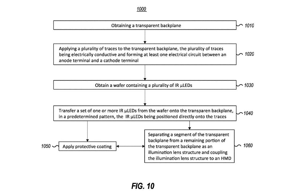
This includes obtaining a transparent substrate, applying multiple traces to a transparent backplane. Wherein the multiple traces are conductive and form at least one circuit between an anode terminal and a cathode terminal.
Then, an infrared μLED wafer is obtained, which contains multiple infrared μLEDs or a material that can be individually extracted as discrete infrared μLEDs with a maximum size of <100 μm. Next, a group of one or more infrared uLEDs are transferred to the substrate in a predetermined pattern, and the infrared uLEDs are electrically coupled to at least one circuit on the backplane/substrate.
Titled "MicroLED based invisible illumination for eye The Microsoft patent application for "tracking" was originally submitted in January 2023 and was recently published by the US Patent and Trademark Office.
It should be noted that, generally speaking, after the US patent application is accepted for review, it will be automatically published 18 months from the application date or priority date, or published within 18 months from the application date at the request of the applicant. Note that the publication of a patent application does not mean that the patent is approved. After the patent application, the US Patent and Trademark Office needs to conduct an actual review, which may take 1 to 3 years.
Contact: David
Phone: +8618665976986
Tel: +8675521563288
Email: [email protected]
Add: 305 Room A Buiding Huafeng International Robot Industrial Park Xixiang Bao'an
 hicenda
 David Dang